
ISL6615A is a high-speed MOSFET driver optimized to drive upper and lower power N-Channel MOSFETs in a synchronous rectified buck converter topology. This driver, combined with an Intersil Digital or Analog multiphase PWM controller, forms a complete high frequency and high efficiency voltage regulator. The ISL6615A drives both upper and lower gates over a range of 4.5V to 13.2V. This drive-voltage provides the flexibility necessary to optimize applications involving trade-offs between gate charge and conduction losses. The ISL6615A features 6A typical sink current for the low-side gate driver, enhancing the lower MOSFET gate hold-down capability during PHASE node rising edge, preventing power loss caused by the self turn-on of the lower MOSFET due to the high dV/dt of the switching node. An advanced adaptive zero shoot-through protection is integrated to prevent both the upper and lower MOSFETs from conducting simultaneously and to minimize the dead-time. The ISL6615A includes an overvoltage protection feature operational before VCC exceeds its turn-on threshold, at which the PHASE node is connected to the gate of the low side MOSFET (LGATE). The output voltage of the converter is then limited by the threshold of the low side MOSFET, which provides some protection to the load if the upper MOSFET(s) is shorted. The ISL6615A also features an input that recognizes a high-impedance.
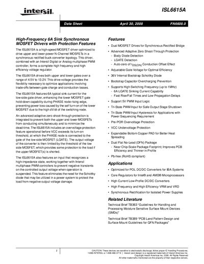
The ISL6615A MOSFET driver from Intersil provides dual high‑side and low‑side gate drive for synchronous rectified buck converters. It supports a wide gate‑drive voltage range (4.5 V‑13.2 V) and delivers up to 6 A typical sink current for the low‑side MOSFET.
Key features include advanced adaptive zero shoot‑through protection, tri‑state PWM input with shutdown window, internal 36 V bootstrap Schottky diode, and a compact DFN package suitable for high‑frequency, high‑efficiency power regulation.
| Typical sink current | 6 A |
|---|---|
| Maximum switching frequency | up to 1 MHz |
| Internal bootstrap diode voltage | 36 V |
| Package type | Dual Flat No‑Lead (DFN) |
| Operating temperature range (plastic package) | -40 °C to +85 °C |
The driver provides a typical sink current of 6 A for the low‑side gate.
The ISL6615A can operate at switching frequencies up to 1 MHz.
Yes, it contains a 36 V internal bootstrap Schottky diode.