
ISL6609, ISL6609A is a high frequency MOSFET driver optimized to drive two N-Channel power MOSFETs in a synchronous-rectified buck converter topology. This driver combined with an Intersil ISL63xx or ISL65xx multiphase PWM controller forms a complete single-stage core-voltage regulator solution with high efficiency performance at high switching frequency for advanced microprocessors. The IC is biased by a single low voltage supply (5V), minimizing driver switching losses in high MOSFET gate capacitance and high switching frequency applications. Each driver is capable of driving a 3nF load with less than 10ns rise/fall time. Bootstrapping of the upper gate driver is implemented via an internal low forward drop diode, reducing implementation cost, complexity, and allowing the use of higher performance, cost effective N-Channel MOSFETs. Adaptive shoot-through protection is integrated to prevent both MOSFETs from conducting simultaneously. The ISL6609, ISL6609A features 4A typical sink current for the lower gate driver, enhancing the lower MOSFET gate hold-down capability during PHASE node rising edge, preventing power loss caused by the self turn-on of the lower MOSFET due to the high dV/dt of the switching node. The ISL6609, ISL6609A also features an input that recognizes a high-impedance state, working together with Intersil multiphase PWM controllers to prevent negative transients on the controlled output.
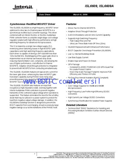
The ISL6609 and ISL6609A drivers are optimized for driving two N‑Channel power MOSFETs in a synchronous‑rectified buck‑converter topology. They operate from a single 5 V bias supply and provide fast rise/fall times, adaptive shoot‑through protection, and a three‑state PWM input.
Key features include 4 A typical sink current, 0.4 Ω on‑resistance, internal bootstrap diode, and support for high‑frequency operation. The datasheet provides ordering information, pin‑outs, absolute maximum ratings, electrical specifications, layout guidelines, and package dimensions for both SOIC and QFN versions.
| BOOT Voltage range | -0.3 V to 25 V (DC) or 36 V (<200 ns) |
|---|---|
| Ambient Temperature Range (operating) | -40 °C to 125 °C |
| Lower gate driver sink current | 4 A typical |
| On‑Resistance | 0.4 Ω |
The lower gate driver can sink up to 4 A typical.
The device is rated for ambient temperatures from –40 °C to 125 °C.
It uses adaptive shoot‑through protection to avoid simultaneous conduction.