
The AT49BV320D(T) is a 2.7 volt 32-megabit flash memory organized as 2,097,152 words of 16 bits each. The memory is divided into 71 sectors for erase operations. The device is offered in a 48-lead TSOP package and a 47-ball CBGA package. The device has CE and OE control signals to avoid any bus contention. This device can be read or reprogrammed using a single power supply, making it ideally suited for in-sys- tem programming. The device powers on in the read mode. Command sequences are used to place the device in other operation modes.
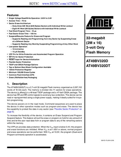
The AT49BV320DT is a 32‑megabit (2M × 16) flash memory offered in 48‑lead TSOP and 47‑ball CBGA packages. It supports single‑voltage read/write operation from 2.65 V to 3.6 V and provides flexible sector protection, erase‑suspend and program‑suspend features.
The document includes pin configurations, block diagram, command sequences, sector protection modes, and timing specifications such as 70 ns access time, 100 ms sector erase time, and 10 µs fast word program time.
| Voltage range (read/write) | 2.65 V to 3.6 V |
|---|---|
| Access time | 70 ns |
| Fast word program time | 10 µs |
| Fast sector erase time | 100 ms |
| Active current | 10 mA |
| Standby current | 15 pA |
| Minimum erase cycles | 100,000 |
| Package options | TSOP and CBGA |
| Memory size | 32 Mbit (2M × 16) |
| Protection register size | 128‑bit |
It operates from 2.65 V up to 3.6 V for both read and write.
It allows an ongoing sector erase to be paused so that other sectors can be read or programmed, then resumed later.
The device offers Softlock and Hardlock modes, which can be set via specific command sequences and optionally combined with the WP pin.