
AT49BV040B is a 2.7V to 5.5V in-system reprogrammable Flash Memory from Atmel. It has 4Mb of memory and is organized as 524,288 words by 8 bits. The read access time is 70 ns (VCC = 2.7V to 3.6V) and 55 ns (VCC = 4.5V to 5.5V). The power dissipation is 72 mW (VCC = 2.7V to 3.6V) and 110 mW (VCC = 4.5V to 5.5V).
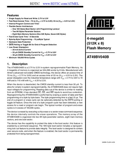
The AT49BV040B is a 4‑megabit (512K × 8) in‑system reprogrammable flash memory that operates from a single 2.7 V to 5.5 V supply. It offers fast read access times of 70 ns (2.7 V‑3.6 V) and 55 ns (4.5 V‑5.5 V), low active current (20 mA) and ultra‑low standby currents (25 pA‑30 pA). The device is organized into a 16 KB boot sector, two 8 KB parameter sectors, and eight main memory sectors ranging from 32 KB to 64 KB.
The datasheet describes the pinout for 32‑lead PLCC, VSOP and TSOP packages, the block diagram of the memory array, and detailed command sequences for read, chip erase, sector erase, byte programming, and boot‑sector lockout. It also explains status monitoring via DATA polling, toggle‑bit detection, and the erase/program status bit, as well as absolute maximum ratings and mechanical dimensions.
| Memory Size | 4 megabit (512 K × 8) |
|---|---|
| Supply Voltage | 2.7 V to 5.5 V |
| Read Access Time | 70 ns (2.7 V‑3.6 V) / 55 ns (4.5 V‑5.5 V) |
| Active Current | 20 mA |
| Write/Erase Endurance | ≥ 100 000 cycles |
| Erase Cycle Time | 8 seconds |
| Boot Sector Size | 16 KB |
It operates from a single supply of 2.7 V to 5.5 V.
The device is rated for a minimum of 100 000 write/erase cycles.
The boot sector is 16 KB, covering addresses 00000 – 003FFFh.
The device provides DATA polling or a toggle‑bit feature to indicate the end of a program or erase cycle.