
This document describes the ADF4001, which is a 200 MHz clock generator PLL. It features a wide bandwidth, programmable charge pump currents, and a 3-wire serial interface.
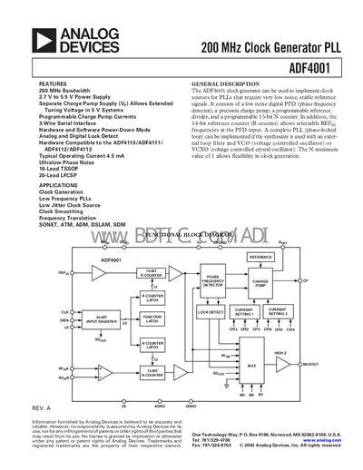
The ADF4001 clock generator provides a low‑noise, stable reference for PLLs, featuring a digital phase‑frequency detector, programmable charge pump, and 13‑bit N counter. It supports a wide range of applications such as clock generation, low‑jitter sources, and frequency translation.
The device is supplied with a 2.7 V‑5.5 V analog power rail, a separate charge‑pump supply, and a 3‑wire SPI‑compatible serial interface. Detailed specifications, pin configurations, timing diagrams, and PCB design guidelines are included for designers.
| RF Input Frequency | 5 – 165 MHz (min/max) |
|---|---|
| Analog Power Supply (AVpp) | 2.7 V – 5.5 V |
| Typical Operating Current | 4.5 mA |
| Phase Noise Floor @ 200 kHz PFD | -161 dBc/Hz (typ) |
| Maximum Serial Clock Rate (SPI) | 20 MHz |
The device draws about 4.5 mA typical operating current.
The phase‑noise floor is –161 dBc/Hz typical at 200 kHz PFD.
The SPI interface can be clocked up to 20 MHz.
AVpp can be between 2.7 V and 5.5 V, with DVpp matching AVpp and Vp up to 6.0 V.