
The ADATE209 is a dual pin driver designed for testing DDR2, DDR3, and DDR4. It can also be used for high speed SoC applica- tions, such as testing PCI Express 1.0 and HDMI™. The device is a three-level driver capable of high fidelity swings from 200 mV to 4 V over a −1 V to +3.5 V range. It has high bandwidth, low power consumption, low EMI, and high resistance to interference.
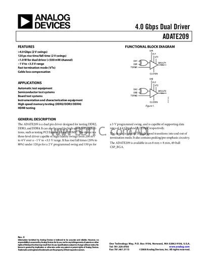
The ADATE209 dual driver provides up to 4.0 Gbps data rates with programmable voltage swings from –1.0 V to +3.5 V and a typical power consumption of less than 1 W. It includes fast termination mode, cable‑loss compensation, and peaking circuitry, making it suitable for DDR2/3/4 memory testing, PCIe, HDMI, and other high‑speed applications.
The device is supplied in a 49‑ball CSP‑BGA package and operates from a +7 V positive supply and –4.5 V negative supply. Electrical specifications include rise/fall times as low as 90 ps for 0.5 V swings, output current limits of 40 mA per pin, and absolute maximum ratings such as +8 V to –5 V supply limits. Detailed pin configurations, functional block diagrams, and thermal resistance data are provided.
| Maximum Data Rate | 4.0 Gbps |
|---|---|
| Rise/Fall Time (0.5 V swing) | 90 ps |
| Supply Voltage Range (Positive) | 0.5 V to +8.0 V |
| Supply Voltage Range (Negative) | –5.0 V to +0.5 V |
| Output Current‑Limit (Source) | 70 mA |
| Package Type | 49‑ball CSP‑BGA |
The ADATE209 supports data rates up to 4.0 Gbps.
The positive supply can range from 0.5 V to +8.0 V, and the negative supply from –5.0 V to +0.5 V.
It is offered in a 49‑ball chip‑scale package (CSP‑BGA).