
AD53500 is a high performance, high output driving capability pin driver, suitable for digital or mixed signal test systems that require high speed and high output driving capability. This product uses a high speed monolithic process and a unique surface mount package to achieve superb electrical performance while maintaining optimum packing density and long-term reliability.
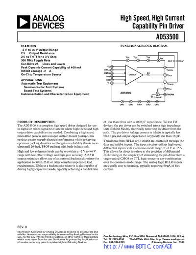
The AD53500 is a complete high‑speed pin driver designed for digital or mixed‑signal test systems that require fast switching and high output drive. It offers a –2 V to +6 V output range, low output resistance, and a 300 MHz toggle rate, making it suitable for automatic test equipment, semiconductor test systems, and board test applications.
The datasheet provides detailed specifications, pin configuration, thermal characteristics, and ordering information. It also includes application notes on power‑supply distribution, bypassing, and current‑limit circuitry, as well as an evaluation‑board schematic and mechanical dimensions for the 20‑lead PSOP package.
| Output Range | -2 V to +6 V |
|---|---|
| Output Resistance | 2.5 Ω |
| Toggle Rate | 300 MHz |
| Peak Dynamic Current Capability | 400 mA |
| Total Supply Range | 16 V |
| Total Power Dissipation | 1.37‑1.54 W |
| Operating Temperature (Junction) | +175 °C |
The AD53500 can toggle at up to 300 MHz.
The total supply range is 16 V, with a positive supply of +10 V and a negative supply of –6 V.
It can provide a peak dynamic current of 400 mA.
The typical output resistance is 2.5 Ω.