
This document describes the features of the RD70HUF2 single-stage amplifier evaluation board, including frequency range, input power, output power, quiescent current, etc.
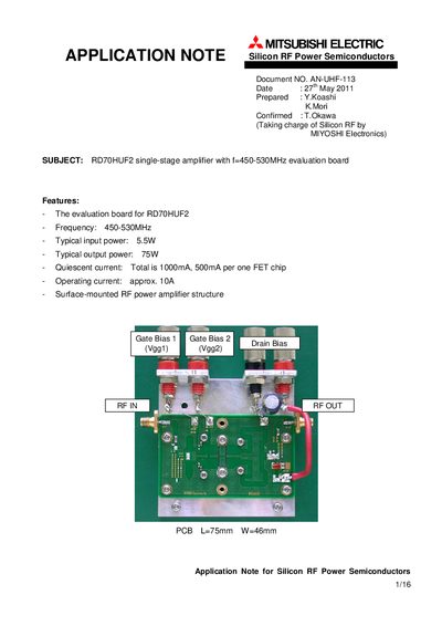
This application note provides detailed information on the RD70HUF2 single‑stage amplifier evaluation board, including its specifications, PCB layout, component list, and thermal design. The board operates in the 450‑530 MHz band with typical input power of 5.5 W and output power of 75 W.
The document also contains equivalent circuitry, land‑pattern dimensions, and performance graphs such as frequency vs. RF power and drain quiescent current. Thermal calculations for the heat sink are included to ensure reliable operation under high‑power conditions.
| Frequency range | 450‑530 MHz |
|---|---|
| Typical input power | 5.5 W |
| Typical output power | 75 W |
| Total quiescent current | 1000 mA |
| Operating current (approx.) | 10 A |
| Board dimensions | 75 mm × 46 mm |
| Substrate total thickness | 1.6 mm |
| Copper thickness (Layer 1 & 4) | 43 µm with gold plating |
| Thermal resistance target for heat sink | < 0.88 °C/W |
The board operates from 450 MHz to 530 MHz.
Typical output power is 75 W.
The total quiescent current is 1000 mA (500 mA per FET chip).
The heat sink should have a thermal resistance much smaller than 0.88 °C/W.