
The XC6206 series are highly precise, low power consumption, 3 terminal, positive voltage regulators manufactured using CMOS and laser trimming technologies. The series provides large currents with a significantly small dropout voltage. The XC6206 consists of a current limiter circuit, a driver transistor, a precision reference voltage and an error correction circuit. The series is compatible with low ESR ceramic capacitors. The currrent limiter's foldback circuit operates as a short circuit protection as well as the output current limiter for the output pin. Output voltages are internally by laser trimming technologies. It is selectable in 0.1V increments within a 1.2V~5.0V range.
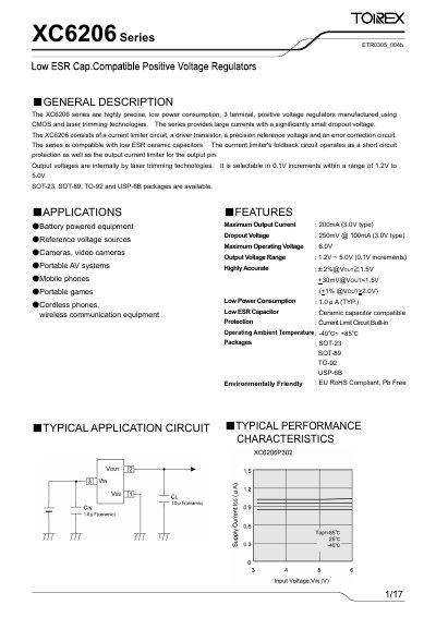
The XC6206 series is designed for battery‑powered equipment, reference voltage sources, cameras, portable AV systems, mobile phones, portable games, cordless phones and other wireless communication devices. It offers high accuracy (±2% or ±1% depending on output voltage), low dropout voltage, built‑in current‑limit protection and compatibility with low‑ESR ceramic capacitors.
Available in SOT‑23, SOT‑89, TO‑92 and USP‑6B packages, the regulator provides up to 500 mA output current, a typical quiescent current of 1.0 µA, and operates from –40 °C to +85 °C. Detailed electrical characteristics, pin configurations and marking rules are included in the datasheet. This manual is written in Chinese.
| Output Voltage Range | 1.2 V ~ 5.0 V (0.1 V increments) |
|---|---|
| Maximum Output Current | 500 mA (SOT‑89) |
| Dropout Voltage | 250 mV @ 100 mA (3.0 V type) |
| Quiescent Current | 1.0 µA typical |
| Available Packages | SOT‑23, SOT‑89, TO‑92, USP‑6B |
| Output Voltage Accuracy | ±2% (VOUT≥1.5 V), ±1% (VOUT>2.0 V) |
The dropout voltage is 250 mV at 100 mA for the 3.0 V type.
The series is offered in SOT‑23, SOT‑89, TO‑92 and USP‑6B packages.
The typical quiescent current is 1.0 µA.
Output voltage can be selected from 1.2 V to 5.0 V in 0.1 V steps.