
The XC6222 series is a highly accurate, low noise, high ripple rejection, low dropout, and low power consumption high speed voltage regulator. The series consists of a voltage reference, an error amplifier, a driver transistor, a current limiter, a thermal protection circuit, and a phase compensation circuit. Over-current protection and thermal protection circuits are integrated. In standby mode, the electric charge at the output capacitor (CL) will be discharged by the internal auto-discharge switch, and as a result the VOUT pin will quickly return to the VSS level.
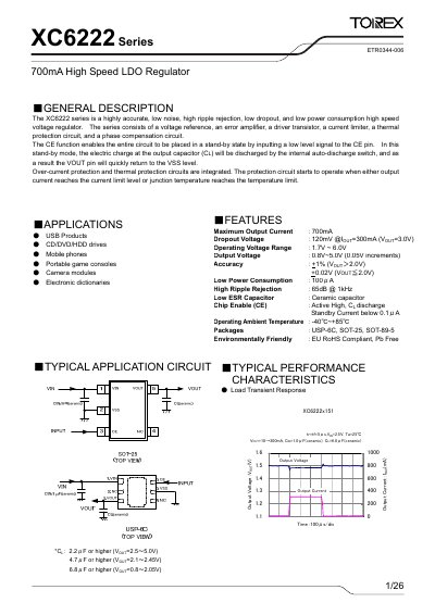
The XC6222 Series LDO regulator provides up to 700 mA output current with a dropout voltage of 120 mV at 300 mA. It operates from 1.7 V to 6.0 V input and delivers adjustable output from 0.8 V to 5.0 V in 0.05 V steps. The device includes a voltage reference, error amplifier, driver transistor, current limiter, thermal shutdown and phase‑compensation circuitry.
The regulator offers CE (chip‑enable) control for standby operation, over‑current and thermal protection, reverse‑current protection, and low standby current (<0.1 µA). Various package options (USP‑6C, SOT‑25, SOT‑89‑5) are available, all RoHS‑compliant.
| Operating Voltage Range | 1.7 V – 6.0 V |
|---|---|
| Output Voltage Range | 0.8 V – 5.0 V (0.05 V increments) |
| Accuracy (VOUT > 2.0 V) | ±1 % |
| Standby Current | < 0.1 µA |
| Package Options | USP‑6C, SOT‑25, SOT‑89‑5 |
It operates with an input voltage from 1.7 V to 6.0 V.
The CE pin enables chip‑enable control; pulling it low puts the device into standby, discharging the output capacitor and reducing standby current.
It includes over‑current protection, thermal shutdown, reverse‑current protection, and a low‑power standby mode.