
The XC6221 series is a high accuracy, low noise, high speed, low dropout CMOS regulator with high ripple rejection. The series includes a reference voltage source, an error amplifier, a current limiter, and a phase compensation circuit. The CE function enables the entire circuit to be in stand-by state by inputting low level signal. As for the XC6221B/D stand-by mode, the electric charge at the output capacitor (CL) will be discharged.
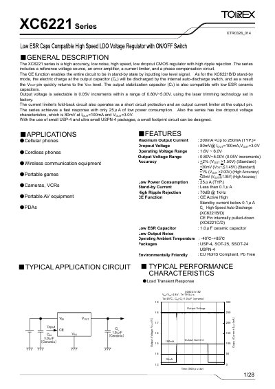
The XC6221 Series is a high‑accuracy, low‑noise, low‑dropout CMOS regulator designed for portable electronic devices such as cellular phones, cameras, and PDAs. It offers selectable output voltages from 0.80 V to 5.00 V in 0.05 V or 0.1 V steps and operates from a 1.6 V to 6.0 V supply.
Key features include a maximum output current of 200 mA, dropout voltage as low as 80 mV at 100 mA load, low standby current (25 µA typ.), high ripple rejection (70 dB @ 1 kHz), and compatibility with low‑ESR ceramic capacitors. The device is offered in USP‑4, SOT‑25, SSOT‑24 and USPN‑4 packages and is RoHS compliant.
| Maximum Output Current | 200 mA (typ.) |
|---|---|
| Dropout Voltage | 80 mV @ I_OUT=100 mA, V_OUT=3.0 V |
| Operating Voltage Range | 1.6 V ~ 6.0 V |
| Low ESR Capacitor Compatibility | 1.0 µF ceramic capacitor |
| Package Types | USP‑4, SOT‑25, SSOT‑24, USPN‑4 |
| Operating Ambient Temperature | -40 °C ~ +85 °C |
| Ripple Rejection | 70 dB @ 1 kHz |
| Input Voltage Range | 1.6 V ~ 6.0 V |
The typical maximum output current is 200 mA, with a typical rating up to 250 mA.
The dropout voltage is 80 mV when I_OUT is 100 mA and V_OUT is 3.0 V.
It is offered in USP‑4, SOT‑25, SSOT‑24, and USPN‑4 surface‑mount packages.
The CE pin enables shutdown; a low signal turns off the internal circuitry, pulling the output to the V_SS level.