
This datasheet provides detailed information on the TC7SH125FS product, including features, absolute maximum ratings, and dimensions.
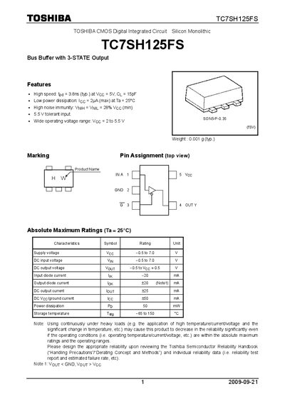
The TC7SH125FS is a CMOS digital integrated circuit bus buffer with 3‑state output, offering high‑speed operation (tpg = 3.8 ns typ.) and low power dissipation (loc = 2 µA max at 25 °C). It features a 5.5 V tolerant input, a wide supply range of 2.0 V to 5.5 V, and high noise immunity.
The device is intended for general electronics applications such as computers, office equipment, measuring equipment, industrial robots, and home electronics. It includes detailed absolute‑maximum ratings, DC and AC electrical characteristics, and package dimensions, along with usage restrictions and reliability guidelines.
| Typical high‑speed propagation delay | 3.8 ns |
|---|---|
| Maximum power dissipation | 50 mW |
| Input voltage (VIN) | 0 V to 5.5 V |
| Typical weight | 0.001 g |
The typical high‑speed propagation delay is 3.8 ns.
The maximum power dissipation is 50 mW.
The input voltage range is 0 V to 5.5 V.