
TPD7102F is a 1-output high-side n-ch power MOS FET gate driver produced by Toshiba. It has a built-in constant current driver and switch power supply output buffer circuit, overvoltage protection, overcurrent protection and thermal protection functions, suitable for high current applications.
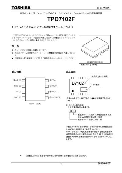
This document describes the TPD7102F, a single‑channel high‑side n‑channel MOSFET gate driver with an integrated charge‑pump. It includes a block diagram, typical application circuit, pinout, timing chart, truth table, and safety notes.
Key sections cover absolute maximum ratings, detailed electrical characteristics, measurement setups, and mechanical dimensions of the surface‑mount package. The datasheet also contains handling guidelines and RoHS compliance information. This manual is written in Japanese.
| Supply voltage (Vpp) | 7 V – 18 V |
|---|---|
| Maximum output sink current (Iout2) | 5 mA |
| Package dimensions | 25.4 mm × 25.4 mm × 0.8 mm |
| Gate‑source diagnostic voltage range (VDIAG) | -0.3 V – 25 V |
The device operates with a supply voltage (Vpp) between 7 V and 18 V.
The maximum output sink current (Iout2) is 5 mA.
The package measures 25.4 mm × 25.4 mm × 0.8 mm.