
This document is an introduction to the SN74AVC8T245 datasheet, which mainly introduces the characteristics of the product, including control inputs, maximum data rates, VCC isolation features, self-locking performance, ESD protection, fully configurable dual-rail design, I/O voltage range, etc.
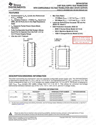
The SN74AVC8T245 provides bidirectional data transfer between two voltage domains (1.2 V‑3.6 V) with independent Vcca and Vccg supplies. It features configurable direction control, 3‑state outputs, and a latch‑up protection scheme that places all I/O ports in high‑impedance when either supply is grounded.
The device supports data rates up to 170 Mbps at low‑voltage operation (Vcca < 1.8 V, Vccg < 1.8 V) and up to 320 Mbps at higher voltages, offers robust ESD protection, and is available in several surface‑mount packages such as QFN‑RHL, TSSOP, and TVSOP.
| Supply voltage range (Vcca / Vccg) | 1.2 V to 3.6 V |
|---|---|
| Maximum data rate (low‑voltage) | 170 Mbps |
| Maximum data rate (high‑voltage) | 320 Mbps |
| ESD protection (Human‑Body Model) | 8000 V |
| Latch‑up current rating | >100 mA |
| Continuous output current | ±50 mA |
| Input clamp current (negative) | -50 mA |
The device can operate at up to 170 Mbps when Vcca and Vccg are below 1.8 V, and up to 320 Mbps at higher supply voltages.
Both Vcca and Vccg can be supplied from 1.2 V to 3.6 V.
It meets 8000‑V Human‑Body Model, 200‑V Machine Model, and 1000‑V Charged‑Device Model specifications.