
Key facts
- Brand
- NXP
- Model
- BLF6G10LS-200
- Category
- Other Electronics
- Documents
- 2
- Languages
- EN
- Last added
- 2012-07-06
Start here
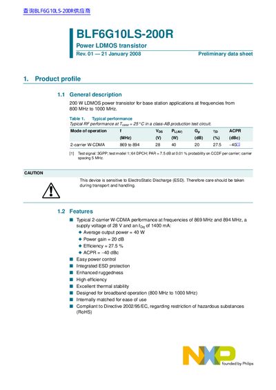
NXP BLF6G10LS-200R Power LDMOS Transistor Preliminary Data Sheet
This document is a preliminary datasheet for the BLF6G10LS-200R Power LDMOS transistor manufactured by NXP Semiconductors. The device is specifically engineered as a 200 W power amplifier for base station applications operating in the frequency range of 800 MHz to 1000 MHz, supporting modes such as GSM, EDGE, W-CDMA, and CDMA.
Read onlineNXP BLF6G10LS-200 specifications
| Average output power (Typical) | 40 W |
|---|---|
| Power gain (Typical) | 20 dB |
| Efficiency (Typical) | 27.5 % |
| ACPR (Typical) | -40 dBc |
Source: NXP BLF6G10LS-200R Power LDMOS Transistor Preliminary Data Sheet
All NXP BLF6G10LS-200 documents by type
Ratings, dimensions and ordering codes, for selection and design work.
Questions answered in these manuals
What is the operating frequency range of this transistor?
The device operates at frequencies from 800 MHz to 1000 MHz.
From: NXP BLF6G10LS-200R Power LDMOS Transistor Preliminary Data Sheet
What is the typical supply voltage for this transistor?
The typical supply voltage (VDS) is 28 V.
From: NXP BLF6G10LS-200R Power LDMOS Transistor Preliminary Data Sheet
What is the maximum drain-source voltage for the BLF6G10LS-200 transistor?
The maximum drain-source voltage is 65 V.
From: NXP BLF6G10LS-200 Power LDMOS Transistor Preliminary Data Sheet
What is the typical power gain of the transistor at 40 W output power?
The typical power gain is 20 dB at an output power of 40 W.
From: NXP BLF6G10LS-200 Power LDMOS Transistor Preliminary Data Sheet