
NXP BLF6G10LS-200 Power LDMOS Transistor Preliminary Data Sheet

The BLF6G10LS-200 is a 200 W LDMOS power transistor from NXP Semiconductors for base station applications at frequencies from 800 MHz to 1000 MHz.
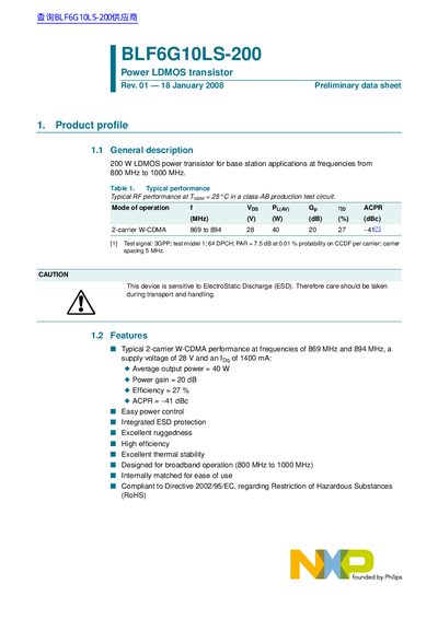

NXP BLF6G10LS-200 Power LDMOS Transistor Preliminary Data Sheet - cover page
Brand
NXP
Category
Other Electronics
Document type
Datasheet
Language
English
Pages
11
File format
PDF
File size
84 KB
Published
06 July, 2012
Updated
30 September, 2023
MD5 checksum
E6338844BFFE2CDEC605CF8A47A03196

About this manual

The document describes the BLF6G10LS-200, a Power LDMOS transistor intended for RF power amplifiers in GSM, EDGE, W-CDMA, and CDMA base stations operating from 800 MHz to 1000 MHz. Key features include typical average output power of 40 W, 20 dB power gain, and efficiency up to 27% at a supply voltage of 28 V.

What's inside

  • Product profile
  • Pinning information
  • Ordering information
  • Limiting values
  • Thermal characteristics
  • Characteristics
  • Application information
  • Test circuit

Specifications

Frequency range800 MHz to 1000 MHz
Average output power40 W
Power gain20 dB
Efficiency27 %

Frequently asked questions

What is the maximum drain-source voltage for the BLF6G10LS-200 transistor?

The maximum drain-source voltage is 65 V.

What is the typical power gain of the transistor at 40 W output power?

The typical power gain is 20 dB at an output power of 40 W.

What is the thermal resistance from junction to case when the case temperature is 80°C?

The thermal resistance from junction to case is 0.34 K/W at a case temperature of 80°C.

Download PDF (84 KB)

More NXP Manuals


View all NXP manuals →