
Key facts
- Brand
- NXP
- Model
- PBSS5350SS
- Industry
- Electronics
- Documents
- 2
- Languages
- EN
- Last added
- 2012-07-03
Start here
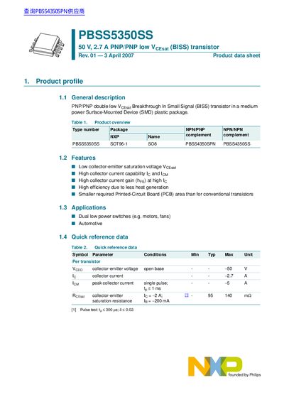
NXP PBSS5350SS 50 V, 2.7 A PNP/PNP Low Vcesat Transistor Product Data Sheet
The PBSS5350SS is a PNP/PNP double low Vce(sat) Breakthrough In Small Signal (BISS) transistor housed in a medium power Surface-Mounted Device (SMD) plastic package. It is designed for applications requiring dual low power switches, such as controlling motors and fans, as well as automotive uses. Key features include low collector-emitter saturation voltage, high collector current capability, and high efficiency due to reduced heat generation.
Read onlineNXP PBSS5350SS specifications
| Collector-emitter voltage (Vceo) | -50 V |
|---|---|
| Collector current (Ic) | -2.7 A |
| Package type | SOT96-1 |
Source: NXP PBSS5350SS 50 V, 2.7 A PNP/PNP Low Vcesat Transistor Product Data Sheet
All NXP PBSS5350SS documents by type
Ratings, dimensions and ordering codes, for selection and design work.
Questions answered in these manuals
What is the maximum collector-emitter voltage?
The maximum collector-emitter voltage is -50 V.
From: NXP PBSS5350SS 50 V, 2.7 A PNP/PNP Low Vcesat Transistor Product Data Sheet
What is the maximum collector current?
The maximum collector current is -2.7 A.
From: NXP PBSS5350SS 50 V, 2.7 A PNP/PNP Low Vcesat Transistor Product Data Sheet
What are the applications of this transistor?
The device is suitable for dual low power switches such as motors and fans, as well as automotive applications.
What is the maximum total power dissipation?
The maximum total power dissipation depends on the PCB material; it is 0.55 W for FR4 and up to 1.43 W for ceramic PCBs.