
This application note explains gate‑drive requirements and design guidelines for the high‑voltage floating‑gate driver IC AN‑978 RevD.
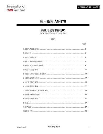
The document provides a comprehensive guide for using the AN‑978 RevD high‑voltage floating‑gate driver IC. It covers gate‑drive voltage requirements, typical circuit topologies, bootstrap component selection, power‑loss calculations, handling of VS negative transients, PCB layout recommendations, and troubleshooting tips.
Key sections include high‑end device gate‑drive requirements, typical structure diagrams, methods to increase gate‑drive current, continuous gate‑drive provision, negative gate‑bias generation, driving buck converters, dual‑active‑bridge and switched‑reluctance motor drives, full‑bridge with current‑mode control, brushless and induction motor drives, push‑pull configurations, high‑end P‑channel operation, and a detailed fault‑diagnosis guide. This manual is written in Chinese.
| Required gate‑drive voltage | 10 V to 15 V above drain |
|---|---|
| Gate current per MOSFET | 0.12 A to 4 A |
| Total power loss (400 V, 100 kHz, no load) | ≈0.534 W |
The gate‑drive voltage must be 10 V to 15 V higher than the drain voltage.
Each MOSFET can source or sink between 0.12 A and 4 A of gate current.
The total power loss is about 0.534 W under those conditions.