
This datasheet describes the 8T49N241, a fractional-feedback PLL frequency translator supporting up to four independent output frequencies from 8kHz to 1GHz.
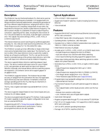
The 8T49N241 is a FemtoClock NG Universal Frequency Translator featuring one fractional-feedback PLL capable of acting as a jitter attenuator and frequency translator. It generates up to four completely independent output frequencies ranging from 8kHz to 1 GHz, which are independent of input reference and crystal frequencies. The device supports various FEC rates, including the new revision of ITU-T Recommendation G.709 (2009), with most conversions having a 0ppm error.
| Output Frequency Range | 8kHz to 1.0GHz (differential) |
|---|---|
| LVCMOS Output Frequency Range | 8kHz to 250MHz |
| Typical Jitter | 0.35ps RMS |
| Operating Temperature Range | -40°C to 85°C |
| Supply Voltage Modes | Full 2.5V or 3.3V, 1.8V support for LVCMOS |
| Package Type | 40-VFQFPN |
The outputs may select among LVPECL, LVDS, HCSL or LVCMOS output levels.
Yes, it supports both automatic and manual hitless reference switching between input clocks.