
IDT54/74FCT16501AT/CT/ET IDT54/74FCT162501AT/CT/ET IDT54/74FCT162H501AT/CT/ET are 18-bit registered bus transceivers with transparent, latched and clocked modes, produced by Integrated Device Technology, Inc.
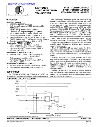
The IDT54/74FCT16501AT/CT/ET family are high‑speed, low‑power 18‑bit CMOS registered bus transceivers that combine D‑type latches and flip‑flops for transparent, latched and clocked data flow. They support live‑insertion, balanced output drive, and optional bus‑hold functionality.
Key features include 0.5 µm CMOS technology, high‑drive outputs (‑32 mA I_OH, 64 mA I_OL), low input leakage (≤ 1 µA), and operation over commercial (‑40 °C to +85 °C) and military (‑55 °C to +125 °C) temperature ranges. Detailed pin configurations, electrical characteristics, and ordering information are provided.
| Technology | 0.5 µm CMOS |
|---|---|
| Output drive (FCT16501AT/CT/ET) | ‑32 mA I_OH, 64 mA I_OL |
| Input leakage | ≤ 1 µA (max) |
| Commercial temperature range | ‑40 °C to +85 °C |
| Military temperature range | ‑55 °C to +125 °C |
| Supply voltage | 5.0 V ± 10 % |
| Input HIGH level (VIH) | 2.0 V |
| Input LOW level (VIL) | 0.8 V |
It provides high‑drive outputs of –32 mA (I_OH) and 64 mA (I_OL).
Yes, it retains the input’s last state during high‑impedance, eliminating the need for external pull‑up/down resistors.
The input leakage is specified as ≤ 1 µA (maximum).