
IS42S16100C1 is ISSI's 16Mb Synchronous DRAM with 200, 166, 143 MHz frequency. It supports two banks simultaneously and independently, LVTTL interface, 4096 refresh cycles every 64 ms, Random column address every clock cycle, Programmable CAS latency (2, 3 clocks), Burst read/write and burst read/single write operations capability, Burst termination by burst stop and precharge command, Byte controlled by LDQM and UDQM, Industrial temperature up to 143 MHz, 400-mil 50-pin TSOP-II, 60-ball fBGA and Lead-free package option.
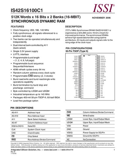
The IS42S16100C1 is a 16‑Mbit (512K × 16 bits × 2 banks) synchronous dynamic RAM offering clock frequencies of 200 MHz, 166 MHz and 143 MHz. It supports programmable burst lengths (1, 2, 4, 8, full page) and CAS latencies of 2 or 3 clocks, with 4096 refresh cycles every 64 ms. The device operates from a single 3.3 V supply and includes LVTTL‑compatible I/O.
The datasheet details pin configurations for 50‑pin TSOP‑II, 60‑ball FBGA and plastic TSOP packages, provides absolute maximum ratings, recommended operating conditions, timing parameters, and packaging dimensions. Electrical characteristics such as supply voltage ranges, leakage currents, and power dissipation are also listed.
| Memory organization | 512K Words × 16 Bits × 2 Banks (16 Mbit) |
|---|---|
| Supply voltage (recommended) | 3.0 V min / 3.3 V typ / 3.6 V max |
| Clock frequency | 200 MHz, 166 MHz, 143 MHz |
| CAS latency | 2 or 3 clocks |
| Refresh cycles | 4096 cycles every 64 ms |
| Operating temperature range | -40 °C to +85 °C (industrial) |
The recommended supply voltage is 3.0 V minimum, 3.3 V typical, and 3.6 V maximum.
It supports clock frequencies of 200 MHz, 166 MHz, and 143 MHz.
The FBGA package uses code B and contains 60 balls (10.1 mm × 6.4 mm, 0.65 mm ball pitch).
The TSOP‑II package has 50 pins.