
This datasheet describes the IDT 85104I, a low skew, high performance 1-to-4 Differential/LVCMOS-to-0.7V HCSL Fanout Buffer.
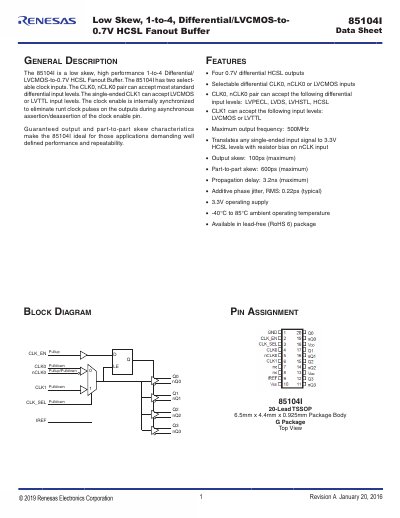
The IDT 85104I is a fanout buffer designed to translate single-ended clock inputs into four differential HCSL outputs with guaranteed low skew and repeatability. It features selectable clock inputs, accepting either a differential pair (CLK0/nCLK0) or a single-ended input (CLK1), allowing flexibility in system design.
| Maximum Output Frequency | 500MHz (CLK_SEL = 0) |
|---|---|
| Output Skew | 100ps maximum |
| Part-to-Part Skew | 600ps maximum |
| Propagation Delay | 3.2ns maximum (CLK_SEL = 0) |
| Operating Supply Voltage | 3.3V |
The CLK0, nCLK0 pair can accept LVPECL, LVDS, LVHSTL, or HCSL differential input levels.
The device supports an ambient operating temperature range of -40°C to 85°C.