
This datasheet provides the dimensions and land pattern recommendations for the Fairchild Semiconductor SOIC-14 package (FS PKG Code S2) conforming to JEDEC…
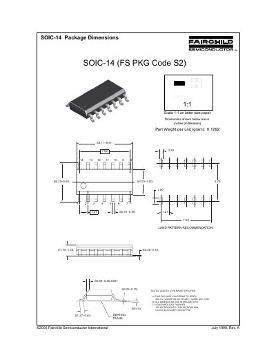
This document details the physical dimensions and land pattern recommendations for the SOIC-14 package, identified by the Fairchild Semiconductor package code S2. The specifications are provided to a 1:1 scale on letter-size paper and include measurements in both inches and millimeters.
| Package Standard | JEDEC MS-012, Variation AB, Issue C |
|---|---|
| Part Weight | 0.1292 grams |
| Lead Finish | 200 microinches / 5.08 microns min. Lead/Tin (Solder) on Copper |
This package conforms to JEDEC MS-012, Variation AB, Issue C, dated May 1990.
The weight per unit is 0.1292 grams.
The standard lead finish is a minimum of 200 microinches or 5.08 microns of lead/tin solder on copper.