
Analog Devices ADSP-BF561 PCM Interface Emulation Application Note

This application note discusses how to emulate the PCM interface using four programmable flag pins (GPIOs) of the ADSP-BF561 Blackfin® processor. This application note applies to designs in which all of the serial interfaces present on the devices are in use and hence the need for emulation of the PCM interface arises.
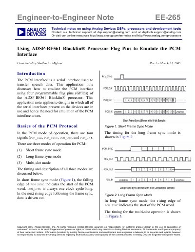

Analog Devices ADSP-BF561 PCM Interface Emulation Application Note - cover page
Brand
Analog Devices
Category
Other Electronics
Document type
Application Note
Language
English
Pages
5
File format
PDF
File size
290 KB
Published
03 August, 2012
Updated
30 September, 2023
MD5 checksum
91BBAE5C4F4DF0B92E1355B42573FB2A

About this manual

The document describes a method to emulate a Pulse Code Modulation (PCM) interface on the ADSP-BF561 Blackfin processor using four programmable flag pins (GPIOs). This solution is intended for designs where all standard serial interfaces are already in use. The emulation supports both transmit and receive operations by utilizing the Serial Port (SPORT) and the flag pins (PF9, PF10, PF11, PF12) to generate clocks, frame syncs, and data signals.

What's inside

  • Introduction
  • Basics of the PCM Protocol
  • Short and Long Frame Sync Implementation
  • Transmit in Short and Long Frame Sync
  • Receive in Short and Long Frame Sync
  • Transmit and Receive in Multi-Slot Mode
  • Clock Frequency Configuration
  • Test Case Implementation

Frequently asked questions

Which four programmable flag pins are used to emulate the PCM interface?

The implementation uses PF9, PF10, PF11, and PF12.

How is the clock generated for transmit in short and long frame sync modes?

The core timer generates an interrupt at a rate twice that of the desired clock rate.

What interrupt rate is required to generate an 8 kHz clock rate?

The interrupt for the timer should be generated at 16 kHz.

Download PDF (290 KB)

More Analog Devices Manuals


View all Analog Devices manuals →