
EPXA1 I/O Pins version 1.6 is a product released by Altera Corporation. It has two packaging forms: 672-Pin FineLine BGA and 484-Pin Fineline BGA. It supports DDR_VS0, DDR_VS1 and other functions.
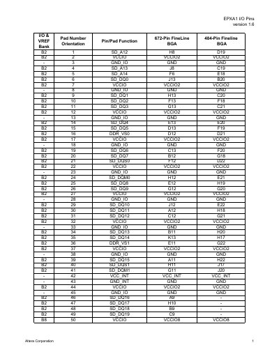
This document serves as a technical reference for the Altera EPXA1 FPGA, specifically focusing on the I/O pin configurations. It provides a comprehensive list of pin assignments across various banks, including power connections (VCCIO, GND_IO) and specific signal functions.
| Pin Count | 672-Pin |
|---|---|
| Alternative Pin Count | 484-Pin |
| Document Version | version 1.6 |
Pin B2-6 functions as SD_DQ0.
VCCIO is at pin B2-7 and GND_IO is at pin B2-8.
Pin B3-304 is VO, CLKUSR(1) and pin B3-305 is VO, RDYnBSY (1).