
Altera HardCopy III Device Family Pin Connection Guidelines

This is an English document, which is the preliminary version of the HardCopy III device family pin connection guidelines released by Altera in 2009.
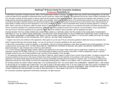

Altera HardCopy III Device Family Pin Connection Guidelines - cover page
Brand
Altera
Category
Other Electronics
Document type
Application Note
Language
English
Pages
9
File format
PDF
File size
325 KB
Published
01 August, 2012
Updated
30 September, 2023
MD5 checksum
467242BD7A211872C2D06CCF87F84104

About this manual

This document serves as a preliminary guide for determining pin connections for the Altera HardCopy III device family. It is intended for use as a recommendation rather than a formal specification and must be verified against the official datasheet for any specific design implementation. The guidelines are provided under a specific license agreement with Altera Corporation.

What's inside

  • Pin Connection Guidelines Agreement
  • Clock and PLL Pins
  • Dedicated Configuration JTAG Pins
  • Pin Description
  • Connection Guidelines

Frequently asked questions

What is the recommended connection for unused Clock and PLL input pins?

Unused Clock and PLL input pins should be connected to GND.

How should the TEMPDIODE pins be connected if the temperature sensing diode is not used?

If the temperature sensing diode is not used, connect the TEMPDIODE pins to GND.

Download PDF (325 KB)

More Altera Manuals


View all Altera manuals →