
The MC10E404/100E404 is a 4-bit differential AND/NAND device. The differential operation of the device makes it ideal for pulse shaping applications where duty cycle skew is critical. Special design techniques were incorporated to minimize the skew between the upper and lower level gate inputs. Because a negative 2-input NAND function is equivalent to a 2-input OR function, the differential inputs and outputs of the device also allow for its use as a fully differential 2 input OR/NOR function. The output RISE/FALL times of this device are significantly faster than most other standard ECLinPS devices resulting in an increased bandwidth. The differential inputs have clamp structures which will force the Q output of a gate in an open input condition to go to a LOW state. Thus, inputs of unused gates can be left open and will not affect the operation of the rest of the device. Note that the input clamp will take affect only if both inputs fall 2.5V below VCC.
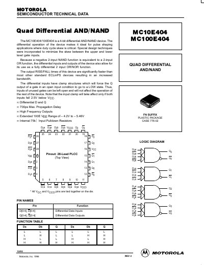
The MC10E404/MC100E404 is a 4-bit differential AND/NAND device designed for pulse shaping applications where duty cycle skew is critical. The device features significantly faster rise and fall times than standard ECLinPS devices, resulting in increased bandwidth.
The maximum propagation delay is 700 ps.
The extended VEE range is -4.2V to 5.46V.