
The MC74AC112/74ACT112 consists of two high-speed completely independent transition clocked JK flip-flops. The clocking operation is independent of rise and fall times of the clock waveform. The JK design allows operation as a D flip-flop (refer to MC74AC74/74ACT74 data sheet) by connecting the J and K inputs together. Asynchronous Inputs: LOW input to SD (Set) sets Q to HIGH level LOW input to CD (Clear) sets Q to LOW level Clear and Set are independent of clock Simultaneous LOW on CD and SD makes both Q and Q HIGH • Outputs Source/Sink 24 mA • ′ACT112 Has TTL Compatible Inputs CP VCC CP1 K1 J1 SD1 Q1 Q1 CD1 CD2 CP2 K2 J2 SD2 CD J Q Q2 SD CONNECTION DIAGRAM Q2 GND 1 2 3 4 5 6 7 8 9 10 11 12 13 14 15 16 K Q CP SD K Q CD J Q MODE SELECT — TRUTH TABLE Operating Mode Inputs Outputs Operating Mode SD CD J K Q Q Set L H X X H L Reset (Clear) H L X X L H *Undetermined L L X X H H Toggle H H h h q q Load “0” (Reset) H H l h L H Load “1” (Set) H H h l H L Hold H H l l q q H, h = HIGH Voltage Level L, l = LOW Voltage Level X = Don’t Care l, h (q) = Lower case letters indicate the state of the referenced input (or output) one set-up time prior to the HIGH to LOW clock transition. *Both outputs will be HIGH while both SD and CD are LOW, but the output states are unpredictable if SD and CD go HIGH simultaneously.
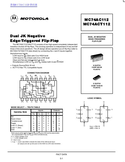
This document provides technical specifications for the Motorola MC74AC112 and MC74ACT112, which are dual JK negative edge-triggered flip-flops. The devices feature high-speed operation with clocking independent of rise and fall times, allowing them to function as D flip-flops when J and K inputs are connected. They include asynchronous Set and Clear inputs and are available in plastic DIP and SOIC packages.
| Outputs Source/Sink Current | 24 mA |
|---|---|
| DC Supply Voltage | -0.5 to +7.0 V |
| Operating Ambient Temperature | -40 to +85 °C |
| Propagation Delay (Typical) | 1.0 ns |
| Input Capacitance | 45 pF |
Yes, by connecting the J and K inputs together.
Both Q and Q outputs will be HIGH.
The typical propagation delay is 1.0 ns.