
The document introduces the query method of BGA suppliers and the characteristics of suppliers
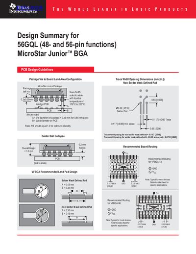
This document provides PCB design guidelines for the MicroStar Junior™ BGA package, specifically covering via-to-board land area configurations and solder mask definitions. It includes recommended trace width/spacing dimensions and board routing strategies for both 48-pin and 56-pin functions to ensure optimum reliability.
The datasheet also details geometric dimensioning and tolerancing (GD&T) terms such as coplanarity and true position, along with ideal IR reflow profiles. Additionally, it presents package reliability data from accelerated life testing, including autoclave, thermal shock, and temperature cycling results.
| Coplanarity | 0.08 mm |
|---|---|
| Position Tolerance | 0.05 mm DIA. |
| Solder Ball Diameter (Max Material) | 0.45 mm DIA. |
| Trace Width/Spacing (Non-Solder Mask Defined) | 0.117 [.0046] |
| Quantity per reel | 1,000 |
The ideal time above 200°C is between 30 and 60 seconds.
TI recommends the use of "no clean" compositions for mounting MicroStar Junior BGAs.