
This document introduces Agilent Technologies' Scanning Microwave Microscope (SMM), a new Scanning Probe Microscope (SPM) that combines the electromagnetic measurement capabilities of a microwave Vector Network Analyzer (VNA) with the nanometer-resolution and Angstrom-scale positioning capabilities of an Atomic Force Microscope (AFM). Agilent VNAs are mature, highly sophisticated characterization instruments that make extremely accurate, calibrated measurements of complex-valued ratios on electromagnetic signals. This measurement capability, delivered to the apex of an AFM tip makes the SMM the only SPM in its class, enabling calibrated, traceable measurements of electrical properties such as impedance and capacitance, with the high spatial resolution.
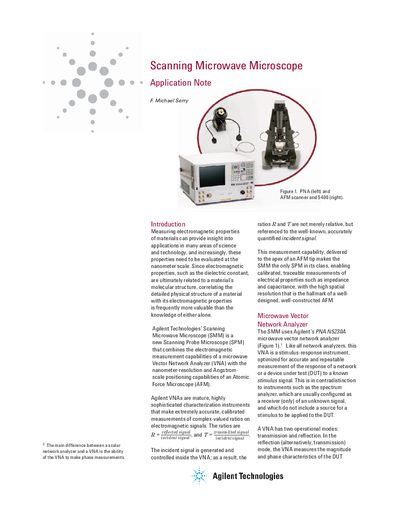
The Agilent Scanning Microwave Microscope (SMM) is a Scanning Probe Microscope that combines the electromagnetic measurement capabilities of a microwave Vector Network Analyzer (VNA) with the nanometer-resolution positioning of an Atomic Force Microscope (AFM). This unique combination enables calibrated, traceable measurements of electrical properties such as impedance and capacitance with high spatial resolution.
The document details the SMM's operation using the Agilent PNA N52304 VNA in reflection mode to measure the impedance of the tip-sample interface. It explains applications such as Scanning Impedance Microscopy and Scanning Capacitance Microscopy (SCM), highlighting how the SMM overcomes limitations of traditional SCM by enabling absolute measurements of carrier densities in semiconductors.
| Operating Frequency Range | 1.5-6 GHz |
|---|---|
| VNA Model | PNA N52304 |
The VNA has the ability to make phase measurements, whereas a scalar network analyzer does not.
The primary application is Scanning Impedance Microscopy, which measures the impedance of the tip-sample interface.
It uses a half-wavelength impedance transformer to place the measurand directly across an external 50 Ohm impedance, allowing for calibrated, traceable measurements.