
intel 28F128J3A 28F640J3A 28F320J3A (x8/x16) 3 Volt Intel StrataFlash Memory Preliminary Datasheet

Intel® StrataFlash™ Memory 28F128J3A, 28F640J3A, 28F320J3A (x8/x16) Preliminary Datasheet
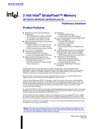

intel 28F128J3A 28F640J3A 28F320J3A (x8/x16) 3 Volt Intel StrataFlash Memory Preliminary Datasheet - cover page
Brand
Intel
Category
Memory
Document type
Datasheet
Language
English
Pages
58
File format
PDF
File size
316 KB
Published
12 June, 2012
Updated
01 October, 2023
Model
X16
MD5 checksum
ABDDE8C7960FC19082D7BA0E828479BB

About this manual

This document is a preliminary datasheet for Intel's 28F128J3A, 28F640J3A, and 28F320J3A (x8/x16) StrataFlash memory devices. These products utilize a high-density symmetrically-blocked architecture with erase blocks of 128 Kbytes in densities ranging from 32 Mbit to 128 Mbit.

What's inside

  • Product Overview
  • Principles of Operation
  • Bus Operations
  • Command Definitions
  • Design Considerations
  • Electrical Specifications
  • Ordering Information

Specifications

Vcc Operation Range2.7 V-3.6 V
Read Access Time (32 M)110/25 ns
Total Min. Erase Cycles (128 Mbit)12.8M
Effective Programming Time6 us per Byte

Frequently asked questions

What is the technology generation of this memory?

The devices utilize Intel's 0.25 micron ETOX™ VI process technology.

What voltage range is required for the 28F128J3A, 28F640J3A, and 28F320J3A memory devices?

These devices operate with a Vcc voltage between 2.7 V and 3.6 V.

What is the minimum number of erase cycles supported by the 128 Mbit, 64 Mbit, and 32 Mbit versions?

The 128 Mbit version supports 12.8M cycles, the 64 Mbit version supports 6.4M cycles, and the 32 Mbit version supports 3.2M cycles.

What is the effective programming time per byte for these memory devices?

The effective programming time is 6 us per byte.

Download PDF (316 KB)

More Intel Manuals


View all Intel manuals →