
The MM74HC574 is a high-speed octal D-type edge-triggered flip-flop that utilizes advanced silicon-gate P-well CMOS technology. It possesses the high noise immunity and low power consumption of standard CMOS integrated circuits, as well as the ability to drive 15 LS-TTL loads. Due to the large output drive capability and the 3-STATE feature, these devices are ideally suited for interfacing with bus lines in a bus organized system. These devices are positive edge triggered flip-flops. Data at the D inputs, meeting the set-up and hold time requirements, are transferred to the Q outputs on positive going transitions of the CLOCK (CK) input. When a high logic level is applied to the OUTPUT CONTROL (OC) input, all outputs go to a high impedance state, regardless of what signals are present at the other inputs and the state of the storage elements.
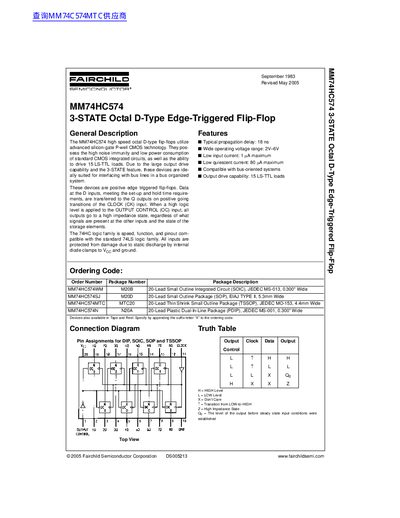
The MM74HC574 is an eight-bit edge-triggered device utilizing advanced silicon-gate P-well CMOS technology. It features high noise immunity and low power consumption while being able to drive up to 15 LS-TTL loads per output pin.
The document provides comprehensive electrical characteristics, including DC and AC parameters across a wide operating voltage range of 2V to 6V. It also includes physical dimensions for various package types such as SOIC, SOP, TSSOP, and PDIP.
| Technology | silicon-gate P-well CMOS technology |
|---|---|
| Noise Immunity | high noise immunity |
| Load Drive Capability | 15 LS-TTL loads |
| Operating Voltage Range | 2V–6V |
| Maximum Input Current | 80µA maximum |
| Typical Propagation Delay | 18 ns |
The typical maximum operating frequency is 60 MHz.
Each output pin can handle a DC current of up to 35 mA.
The data must be stable for at least 10 ns before the clock edge.