
This document describes the design applications, features, and characteristics of the 5 G D S J210 J211 J212 N-Channel RF Amplifier. It is suitable for HF/VHF mixer/amplifier and applications requiring sufficient gain and low noise for sensitive receivers.
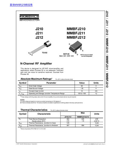
This document provides technical specifications and characteristics for the MMBFJ210, MMBFJ211, and MMBFJ212 series of N-Channel RF Amplifiers. These devices are specifically designed for HF/VHF mixer/amplifier applications where standard processes may not be adequate, offering sufficient gain and low noise performance.
| Package Type | SOT-23 |
|---|---|
| Drain-Gate Voltage (Max) | 25 V |
| Gate-Source Voltage (Max) | -25 V |
| Forward Gate Current (Max) | 10 mA |
| Operating Junction Temperature Range | -55 to +150 °C |
| Total Device Dissipation (J210-212) | 350 mW |
The absolute maximum rating for both the Drain-Gate Voltage and Gate-Source Voltage is 25 V.
The device operates within a junction temperature range of -55 to +150 °C.
The MMBFJ210 has a maximum total device dissipation of 350 mW when mounted on an FR-4 PCB.