
TMS320C5x and TMS320LC5x are digital signal processors with a powerful 16-bit TMS320C5x CPU. They have a single-cycle instruction execution time of 20, 25, 35, and 50 ns for 5V operation, and 25, 40, and 50 ns for 3V operation. They also feature single-cycle 16x16-bit multiply/add, a maximum addressable external memory space of 224Kx16-bit, on-chip program ROM with sizes ranging from 2K to 32Kx16-bit, on-chip program/data RAM (SARAM) with sizes ranging from 1K to 9Kx16-bit, on-chip dual-access program/data RAM (DARAM) with a size of 1K, full-duplex synchronous serial port for coder/decoder interface, time-division-multiplexed (TDM) serial port, hardware or software wait-state generation capability, on-chip timer for control operations, repeat instructions for efficient use of program space, buffered serial port, host port interface, multiple phase-locked loop (PLL) clocking options (x1, x2, x3, x4, x5, x9 depending on the device), block moves for data/program management, on-chip scan-based emulation logic, boundary scan, and five packaging options. It also has low power dissipation and power-down modes, consuming 47 mA (2.35 mA/MIP) at 5V and 40 MHz.
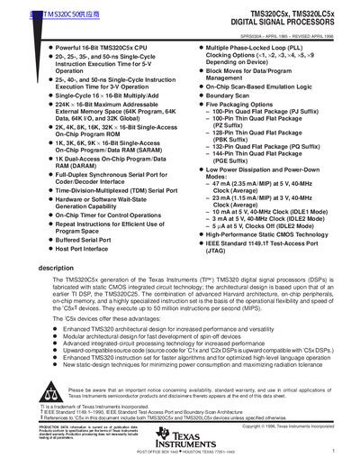
This document provides a comprehensive overview of the TMS320C5x generation of Digital Signal Processors (DSPs) from Texas Instruments. The devices are fabricated with static CMOS technology and feature an enhanced Harvard architecture based on the earlier TMS320C25 design. Key capabilities include powerful 16-bit CPU performance, single-cycle instruction execution times ranging from 20 to 50 nanoseconds depending on voltage and device speed, and a specialized instruction set optimized for high-level language operation.
| CPU Architecture | Powerful 16-Bit TMS320C5x CPU |
|---|---|
| Instruction Execution Time (5V) | 20-, 25-, 35-, and 50-ns Single-Cycle |
| Instruction Execution Time (3V) | 25-, 40-, and 50-ns Single-Cycle |
| Multiply/Add Capability | Single-Cycle 16 x 16-Bit Multiply/Add |
| External Memory Space | 224K x 16-Bit Maximum Addressable |
| On-Chip Program ROM | 2K, 4K, 8K, 16K, 32K x 16-Bit Single-Access |
| On-Chip SARAM | 1K, 3K, 6K, 9K x 16-Bit Single-Access |
| On-Chip DARAM | 1K Dual-Access On-Chip Program/Data RAM |
| Power Dissipation (Average) | 47 mA at 5 V, 40-MHz Clock |
| Technology | High-Performance Static CMOS Technology |
They execute up to 50 million instructions per second (MIPS).
Yes, source code for 'C1x and 'C2x DSPs is upward compatible with 'C5x DSPs.
Multiple Phase-Locked Loop (PLL) Clocking Options including x1, x2, x3, x4, x5, and x9 depending on the device.