
The ADN2807 is a 155/622 Mb/s clock and data recovery IC with integrated limiting amp that meets SONET requirements for jitter transfer/ generation/tolerance.
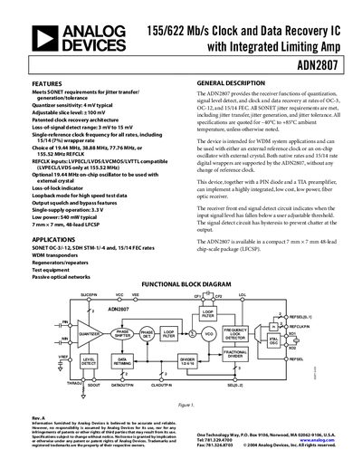
The ADN2807 is a high-speed Clock and Data Recovery (CDR) Integrated Circuit designed for SONET OC-3/-12, SDH STM-1/-4, and 15/14 FEC rates. It features patented clock recovery architecture to meet strict jitter transfer, generation, and tolerance specifications. The device supports both native rates and digital wrappers without changing the reference clock frequency.
| Supply Voltage | 3.0 V to 3.6 V |
|---|---|
| Power Supply Current | 150 mA typical |
| Package Type | 7 mm x 7 mm, 48-lead LFCSP |
| Operating Temperature Range | -40°C to +85°C |
| Jitter Transfer Bandwidth (OC-12) | 140 kHz typical |
All specifications are quoted for an ambient temperature range of -40°C to +85°C.
The device has a typical low power consumption of 540 mW.
The device is available in a compact 7 mm x 7 mm 48-lead chip-scale package.