
The ADN2812 is a Clock and Data Recovery IC with Integrated Limiting Amplifier, supporting a continuous rate of 12.3 Mb/s to 2.7 Gb/s. It exceeds SONET requirements for jitter transfer/generation/tolerance and features adjustable slice level, no reference clock requirement, low power consumption, etc.
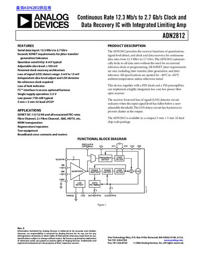
The ADN2812 is a Continuous Rate 12.3 Mb/s to 2.7 Gb/s Clock and Data Recovery IC with an Integrated Limiting Amplifier manufactured by Analog Devices. It provides receiver functions including quantization, signal level detection, and clock and data recovery for continuous data rates without requiring an external reference clock.
The device meets all SONET requirements for jitter transfer, generation, and tolerance. It features a patented clock recovery architecture, adjustable slice level, and independent loss of signal (LOS) detection. The ADN2812 is available in a compact 5 mm x 5 mm 32-lead LFCSP package and operates on a single 3.3 V supply.
| Data Rate | 12.3 Mb/s to 2.7 Gb/s |
|---|---|
| Operating Temperature Range | -40°C to +85°C |
| Supply Voltage | 3.3 V |
| Supply Current | 235 mA typical |
| Package | 5 mm x 5 mm 32-lead LFCSP |
| Jitter Generation (OC-48) | 0.002 UI rms |
No, the device automatically locks to all data rates without the need for an external reference clock or programming.
The typical power supply current is 235 mA.
The loss of signal detect range is 3 mV to 15 mV.