
ADN2807 Rev. A is a 155/622 Mb/s clock and data recovery IC with integrated limiting amp, which meets SONET requirements for jitter transfer/generation/tolerance.
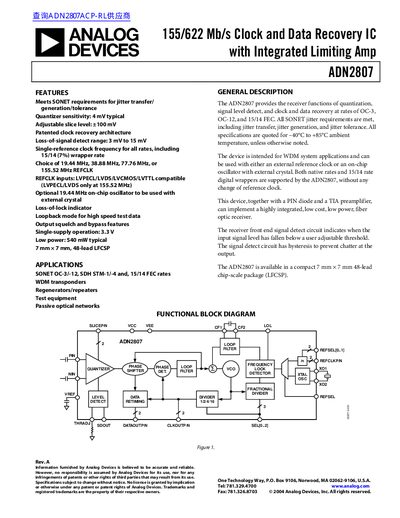
The ADN2807 is a high-speed Clock and Data Recovery (CDR) Integrated Circuit designed to meet SONET requirements for jitter transfer, generation, and tolerance. It supports rates up to OC-12 and 15/14 FEC, featuring an adjustable slice level, loss-of-signal detection, and a choice of reference clock frequencies including an optional on-chip oscillator.
| Quantizer Sensitivity | 4 mV typical |
|---|---|
| Power Supply Voltage | 3.0 V to 3.6 V |
| Operating Temperature Range | -40°C to +85°C |
| Package Type | 7 mm x 7 mm, 48-lead LFCSP |
| Jitter Transfer Bandwidth (OC-12) | 140 kHz to 200 kHz |
The device supports OC-3, OC-12, and 15/14 FEC rates.
Yes, it offers an optional 19.44 MHz on-chip oscillator to be used with an external crystal.
The device has a low power consumption of 540 mW typical.