
The ADN2811 is an OC-48/OC-48 FEC clock and data recovery IC with integrated limiting amp.
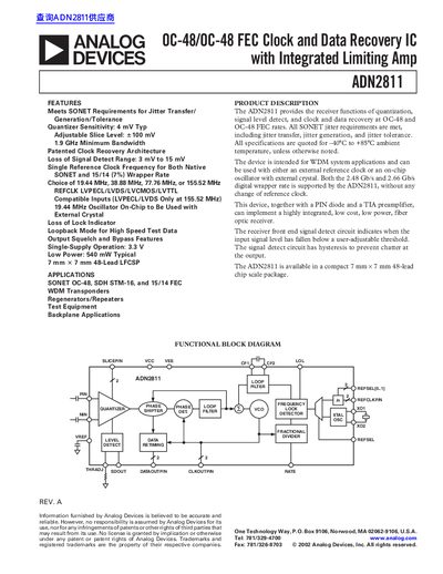
The ADN2811 is a receiver function IC designed to provide quantization, signal level detection, and clock and data recovery at OC-48 and OC-48 Forward Error Correction (FEC) rates. It meets all SONET jitter requirements, including jitter transfer, generation, and tolerance. The device supports both 2.48 Gb/s and 2.66 Gb/s digital wrapper rates without changing the reference clock.
| Upper -3 dB Bandwidth | 1.9 GHz |
|---|---|
| Quantizer Sensitivity | 4 mV Typ |
| Supply Voltage | 3.0 to 3.6 V |
| Operating Temperature Range | -40°C to +85°C |
| Package Type | 7 mm x 7 mm 48-Lead LFCSP |
The device provides receiver functions at OC-48 and OC-48 FEC rates.
Yes, it can be used with either an external reference clock or an on-chip oscillator with an external crystal.
The typical differential output swing (Vodiff) is 910 mV.