
ADN2809 is a multi-rate to 2.7Gbps clock and data recovery IC with limiting amplifier for SONET OC-3/12/48, SDH STM-1/4/16, and all associated FEC rates. It features a patented clock recovery architecture for low power and low jitter.
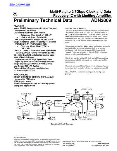
The ADN2809 is a Multi-Rate to 2.7Gbps Clock and Data Recovery IC with a Limiting Amplifier. It meets SONET requirements for jitter transfer, generation, and tolerance. The device supports rates including OC-3, OC-12, OC-48, Gigabit Ethernet, and associated FEC rates, utilizing a single reference clock frequency.
The IC is designed for applications such as WDM transponders, SONET/SDH regenerators, test equipment, and backplane systems. It features a quantizer with adjustable slice levels, a loss of signal detect range, and output squelch functions. The device operates on a single 3.3V supply and is available in a 7x7mm 48-pin LFCSP package.
| Maximum Data Rate | 2.7Gbps |
|---|---|
| Quantizer Sensitivity | 6 mV typical |
| Adjustable Slice Level | +/- 100 mV |
| Minimum Bandwidth | 1.9GHz |
| Supply Voltage | 3.3 Volts |
| Typical Power Consumption | 780 mW |
| Package Type | 48 pin LFCSP |
| Operating Temperature Range | -40 to +85°C |
The device supports SONET OC-3/12/48, SDH STM-1/4/16, Gigabit Ethernet, and all associated FEC rates.
No, a single reference clock frequency is used for all rates, including 15/14 wrapper rates.
The input sensitivity is 6 mV peak-to-peak differential with a bit error rate of less than 1 x 10^-10.