
This document describes the features and characteristics of the Si5435DC P-Channel MOSFET, including maximum ratings, temperature range, and thermal resistance.
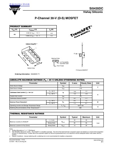
The document details the Si5435DC, a leadless ChipFET package P-Channel MOSFET with a drain-source voltage rating of 30V. Key electrical parameters include an on-state resistance (rDS(on)) ranging from 0.042 to 0.080 ohms and a continuous drain current capability up to 5.6A at 25°C.
| Drain-Source Voltage (VDS) | -30 V |
|---|---|
| Continuous Drain Current (ID) @ TA=25°C | 5.6 A |
| Maximum Power Dissipation (TA=25°C) | 2.5 W |
| Operating Junction Temperature Range | -55 to 150 °C |
| Package Type | 1206-8 ChipFE Tt D D D GD D D S1S G D P-Channel MOSFETBottom ViewMarking Code BE XX Lot Traceability and Date Code Part # Code Ordering Information: Si5435DC-T1 ABSOLUTE MAXIMUM RATINGS (T A=2 5_C UNLESS OTHERWISE NOTED) Parameter Symbol 5 secs Steady State Unit Drain-Source Voltage VDS -- 3 0 V Gate-Source Voltage VGS 20V ContinuousDrainCurrent(TJ=150_C)aTA=2 5_C ID-- 5 . 6 -- 4 . 1 Continuous DrainCurren t(TJ=150_C)a TA=8 5_CID -- 4 . 0 -- 2 . 9A Pulsed Drain Current IDM -- 3 0A Continuous Source Currenta IS -- 2 . 1 -- 1 . 1 MaximumPowerDissipationaTA=2 5_C PD2.5 1.3 W Maximum Power Dissipationa TA=8 5_CPD1.3 0.7W Operating Junction and Storage Temperature Range TJ,Tstg - -55 to 150 _CSoldering Recommendations (Peak Temperature)b, c 260_C THERMAL RESISTANCE RATINGS Parameter Symbol Typical Maximum Unit Mi J titAbitat≤5s e c R40 50 Maximum Junction-to-Ambienta Steady StateRthJA80 95 _C/W Maximum Junction-to-Foot (Drain) Steady State RthJF 15 20C/ Notes a. Surface Mounted on 1" x 1" FR4 Board. b. See Reliability M anual for profile. The ChipFET is a leadless package. The end of the lead terminal is exposed copper (not plated) as a result of the singulation process in manufacturing. A solder f illet at the exposed c opper tip cannot be guaranteed and is not required to ensure adequate bottom side solder intercon- nection. c. Rework Conditions: manual soldering with a soldering iron is not recommended for leadless components. gåâSI5435DCO^UF |
The typical maximum junction-to-ambient thermal resistance (RthJA) is 80 °C/W.
The static gate threshold voltage (VGS(th)) ranges from -2.5 V to -1 V under test conditions of VDS=VGS and ID=-250 mA.
Yes, the ChipFET is described as a leadless package with exposed copper at the end of the lead terminal.