
This document is a copyright statement for ICminer.com Electronic-Library Service, repeated multiple times without providing any specific content.
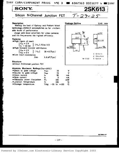
The document describes the Sony 2SK613, a Silicon N-Channel Junction Field Effect Transistor (FET) designed for high efficiency in applications such as head amplifiers for video cameras. Key features include a high figure of merit and low input capacitance.
The datasheet details absolute maximum ratings including drain to gate voltage, source to gate voltage, and junction temperature. It also provides comprehensive electrical characteristics tables with typical values for parameters like forward transfer admittance and input capacitance across different sub-classifications (2SK613-2 through 4).
| Device Type | Silicon N-Channel Junction FET |
|---|---|
| Drain Current (Id) | 50 mA |
| Junction Temperature (Tj) | 150 °C |
It ensures the highest efficiency when used with head amplifiers for video cameras and similar applications.
The absolute maximum rating for allowable power dissipation is 150 mW.
The absolute maximum rating for junction temperature is 150 °C.