
The document introduces the three SRAMs, CY7C1470V33, CY7C1472V33 and CY7C1474V33. They support 250MHz bus operation and have 3.3V/2.5V power supply. They also support single byte write operation.
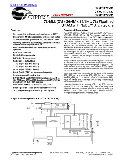
The document details the Cypress Semiconductor CY7C1470V33, CY7C1472V33, and CY7C1474V33 synchronous pipelined burst SRAMs. These devices are designed to support unlimited true back-to-back Read/Write operations with no wait states, utilizing advanced No Bus Latency (NoBL) logic.
| Memory Capacity | 2M x 36 / 4M x 18 / 1M x 72 |
|---|---|
| Operating Voltage | Single 3.3V power supply |
| Max Access Time (250 MHz) | 3.0 ns |
| Max Operating Current | 500 mA |
The devices support bus operations up to 250 MHz.
Yes, they are pin-compatible and functionally equivalent to ZBT devices.