
The ICS650-27 is a low cost, low jitter, high performance clock synthesizer for networking applications. Using analog Phase-Locked Loop (PLL) techniques, the device accepts a 12.5 MHz or 25 MHz clock or fundamental mode crystal input to produce multiple output clocks for networking chips, PCI devices, SDRAM, and ASICs. The ICS650-27 outputs all have zero ppm synthesis error. The ICS650-27 is pin compatible and functionally equivalent to the ICS650-07. It is a performance upgrade and is recommended for all new 3.3V designs.
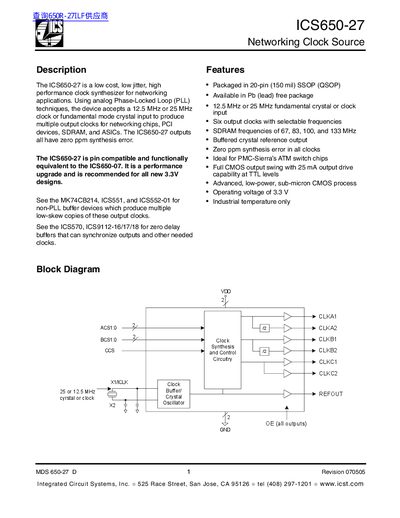
The ICS650-27 networking clock source provides a low‑jitter, high‑performance clock synthesizer for networking applications. It accepts a 12.5 MHz or 25 MHz fundamental crystal or clock input and offers six selectable output clocks, including SDRAM frequencies up to 133 MHz, all with zero‑ppm synthesis error.
The device is supplied in a 20‑pin (150 mil) SSOP package, requires minimal external components such as 0.01 µF decoupling capacitors, and operates from a 3.3 V supply over an ambient temperature range of –40 °C to +85 °C. Detailed pin assignments, electrical characteristics, and ordering information are provided.
| Supply Voltage (typical) | 3.3 V |
|---|---|
| Input Frequency range | 12.5 MHz – 27 MHz |
| SDRAM output frequencies | 67, 83, 100, 133 MHz |
| Operating Temperature | -40 °C to +85 °C |
| Package type | 20‑pin (150 mil) SSOP |
| Output drive capability | 25 mA |
| Decoupling capacitor value | 0.01 µF |
A 0.01 µF decoupling capacitor should be placed between each VDD and GND pin.
The typical supply voltage is 3.3 V (range 3.0 V to 3.6 V).
It provides a full CMOS output swing with a 25 mA drive capability at TTL levels.