
This document describes the features and characteristics of TMS320LF2407, TMS320LF2406, and TMS320LF2402 chips. These chips utilize high-performance static CMOS technology and feature low-power 3.3V design and high performance. The chips have integrated Flash EEPROM, data/program RAM, dual-access RAM, and single-access RAM. Additionally, the chips have two event manager modules for pulse-width modulation control, external event capture, and other functionalities. They are suitable for various motor control applications including AC induction motors, brushless DC motors, switched reluctance motors, and stepper motors.
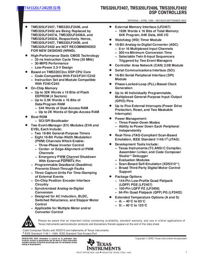
This datasheet describes the TMS320LF2407, TMS320LF2406, and TMS320LF2402 DSP controllers, part of the TMS320C24x™ generation. It outlines the device architecture, core CPU, memory options, and integrated peripherals such as PWM, ADC, CAN, SCI, and SPI modules.
The document includes functional block diagrams, pin‑function tables, memory maps, absolute maximum ratings, recommended operating conditions, mechanical drawings, and revision history. It also notes that these parts are not recommended for new designs and have been superseded by the LF240xA family.
| DSP Core | C2xx |
|---|---|
| Instruction Cycle | 33 ns |
| Performance | 30 MIPS (30 MHz) |
| Boot ROM | Yes |
| External Memory Interface | Yes |
| 10‑bit ADC | Yes, 16 channels, 500 ns min conversion |
| ADC Conversion Time (minimum) | 500 ns |
| SPI Interface | Yes |
| CAN 2.0B Module | Yes |
| Supply Voltage | 3.3 V |
No, the TMS320LF2407, TMS320LF2406, and TMS320LF2402 are not recommended for new designs (NRND).
The 10‑bit ADC has a minimum conversion time of 500 ns.
They operate from a 3.3 V supply.