
This is a high precision, wide bandwidth, high output drive capability CMOS single supply rail to rail operational amplifier
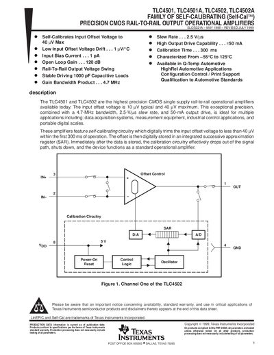
The TLC4501/TLC4502 family provides high‑precision, single‑supply, rail‑to‑rail operational amplifiers featuring self‑calibrating circuitry that trims input offset voltage to less than 40 µV within 300 ms. They deliver a typical slew rate of 2.5 V/µs, a gain‑bandwidth product of 4.7 MHz, and can drive up to ±50 mA into capacitive loads.
The datasheet lists absolute‑maximum ratings, recommended operating conditions, and detailed electrical characteristics for each device variant. Multiple package options are offered (D, JG, U, FK) with mechanical dimensions and hermetic sealing options. A warranty notice and critical‑application disclaimer conclude the document.
| Input offset voltage (typical) | 10 µV |
|---|---|
| Input offset voltage (maximum) | 40 µV |
| Gain‑bandwidth product | 4.7 MHz |
| High‑output drive capability | ±50 mA |
| Calibration time | 300 ms |
| Input bias current | 1 pA |
The self‑calibration circuitry completes trimming in 300 ms at 25 °C.
They can source or sink up to ±50 mA into capacitive loads.
The family is offered in D, JG, U, and FK ceramic dual‑flatpack packages.
Typical input offset voltage is 10 µV.