
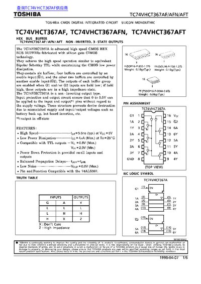
The TC74VHCT367A series are high‑speed CMOS hex‑bus buffers with non‑inverting, 3‑state outputs. Each device contains six buffers; four are controlled by enable input G1 and two by G2. When the enable inputs are low the corresponding buffers are active, otherwise the outputs are high‑impedance.
The datasheet lists absolute maximum ratings, recommended operating conditions, DC and AC electrical characteristics, noise performance, and package dimensions for SOP‑16 and TSSOP‑16 variants. Key parameters include a typical propagation delay of 5.5 ns, low power dissipation of about 4 µA, and a supply voltage range of –0.5 V to 7.0 V.
| Supply Voltage Range | -0.5 V to 7.0 V |
|---|---|
| Typical Propagation Delay | 5.5 ns |
| Low Power Dissipation (typ.) | 4 µA at 25 °C |
| Number of Buffers | 6 |
| Package Weight (SOP‑16, 300 mil) | 0.18 g (typ.) |
The device can operate with a supply voltage from –0.5 V to 7.0 V.
Each TC74VHCT367A contains six buffers.
The typical propagation delay is 5.5 ns.
The part is offered in SOP‑16 (300 mil and 150 mil) and TSSOP‑16 packages.