
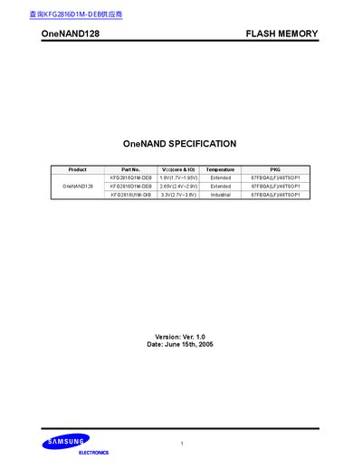
This document provides specifications and features of OneNAND128 flash memory, including the product model, operating voltage, temperature range, and package type.
OneNAND128 is a single‑die flash memory chip that combines a standard NOR‑Flash interface with a NAND‑Flash array. It includes 3 KB of internal BufferRAM (1 KB BootRAM and 2 KB DataRAM) and operates with a 16‑bit host interface at up to 54 MHz.
The device is offered in 1.8 V, 2.65 V, and 3.3 V versions, supports synchronous burst reads, asynchronous reads and writes, and provides features such as OTP area, write protection, and built‑in ECC/ECC. It is available in 67‑ball FBGA and 48‑pin TSOP1 packages and is rated for 100 k program/erase cycles with a 10‑year data retention.
| Design Technology | 0.12 µm |
|---|---|
| Operating Voltage (1.8 V version) | 1.7 V–1.95 V |
| Operating Voltage (2.65 V version) | 2.4 V–2.9 V |
| Operating Voltage (3.3 V version) | 2.7 V–3.6 V |
| Host Interface | 16‑bit |
| Internal BufferRAM | 3 KB (1 KB BootRAM, 2 KB DataRAM) |
| Page Size | 1 KB + 32 bytes |
| Block Size | 64 KB + 2 KB |
| Maximum Clock Frequency | 54 MHz |
| Random Read Access Time | 76 ns |
| Standby Current (1.8 V) | 10 µA |
| Endurance | 100 k program/erase cycles |
| Data Retention | 10 years |
The device is offered in three versions: 1.8 V (1.7 V–1.95 V), 2.65 V (2.4 V–2.9 V), and 3.3 V (2.7 V–3.6 V).
The OneNAND128 can operate at clock frequencies up to 54 MHz.
The device is rated for 100 k program/erase cycles and a data retention period of 10 years.