
The MRF6S27050HR3 is a RF power field effect transistor produced by Freescale Semiconductor. It is suitable for CDMA base station applications with frequencies from 2500 to 2700 MHz.
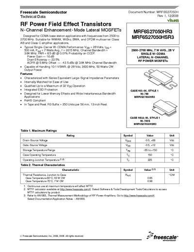
The MRF6S27050HR3 and MRF6S27050HSR3 are N‑channel lateral MOSFETs designed for CDMA base‑station applications in the 2500‑2700 MHz range. They are suitable for WiMAX, WiBro, BWA and OFDM multicarrier Class AB and Class C amplifier designs.
The document provides maximum ratings, thermal characteristics, electrical parameters, test circuit schematics and typical performance graphs, along with revision history and related application notes.
| Drain‑Source Voltage (Vpss) max | +68 Vde |
|---|---|
| Gate‑Source Voltage (Ves) max | +12 Vde |
| Power Gain | 16 dB |
| Drain Efficiency | 22.5 % |
| ACPR @ 5 MHz offset | -42.5 dBc |
| Storage Temperature Range | -65 °C to +150 °C |
| Maximum Junction Temperature | 225 °C |
The device can handle up to +68 Vde drain‑source voltage.
Typical power gain is 16 dB.
Yes, the device is RoHS compliant.