
CDC2510 is a 3.3V low-skew low-jitter phase-lock loop clock driver designed for synchronous DRAM applications. It uses a PLL to precisely align, in both frequency and phase, the feedback (FBOUT) output to the clock (CLK) input signal. The CDC2510 operates at 3.3V VCC and provides integrated series-damping resistors that make it ideal for driving point-to-point loads. A bank of ten outputs provides ten low-skew, low-jitter copies of CLK. Output signal duty cycles are adjusted to 50 percent, independent of the duty cycle at CLK. All outputs can be enabled or disabled via a single output enable input. When the G input is high, the outputs switch in phase and frequency with CLK; when the G input is low, the outputs are disabled to the logic-low state. Unlike many products containing PLLs, the CDC2510 does not require external RC networks. The PLL's loop filter is included on-chip, minimizing power consumption and cost.
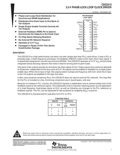
The CDC2510 is a high‑performance, low‑skew, low‑jitter PLL clock driver designed for synchronous DRAM systems. It operates from a 3.3 V supply and provides ten clock outputs that copy the input clock with 50 % duty cycle.
The device includes on‑chip series‑damping resistors, requires no external RC network, and features a 7 ms stabilization time to achieve phase lock after power‑up. It is supplied in a 24‑pin plastic thin‑shrink (PW) package and is qualified for operation from 0 °C to 70 °C.
| Clock frequency range | 25 MHz – 125 MHz |
|---|---|
| Operating temperature range | 0 °C – 70 °C |
| High‑level input voltage (VIH) | 2 V |
| Low‑level input voltage (VIL) | 0.8 V |
The CDC2510 is qualified for operation from 0 °C to 70 °C.