
This document is about the SN74LVC3G04 triple inverter. It is designed for 1.65-V to 5.5-V VCC operation and has a maximum tpd of 4.1 ns. At 3.3 V, the output drive current can reach ±24 mA and it supports partial power-down mode operation.
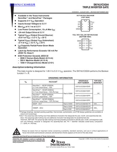
The SN74LVC3G04 triple inverter gate provides three independent inverting buffers that operate from 1.65 V to 5.5 V. It offers low power consumption, a typical propagation delay of 4.1 ns at 3.3 V, and up to +24 mA output drive current.
The device is offered in NanoStar™ and NanoFree™ wafer‑level ball‑grid array (WBGA) packages as well as DCT and DCU small‑outline packages. Mechanical drawings, thermal data, and package dimensions are provided for each variant.
| Output drive current | +24 mA at 3.3 V |
|---|---|
| Propagation delay (tpg) | 4.1 ns at 3.3 V |
| ESD protection (Human‑Body Model) | 2000 V |
| Supply voltage range | 1.65 V to 5.5 V |
The device operates from 1.65 V up to 5.5 V.
It can source up to +24 mA when powered at 3.3 V.
The part meets 2000 V Human‑Body, 200 V Machine, and 1000 V Charged‑Device model specifications.